OTIS home page of the ASIC lab Heidelberg
 |
Content
What is OTIS?
OTIS is an acronym for Outer tracker Time Information System. Actually, it is a chip developed for the LHCb experiment at the LHC (Large Hardron Collider) at CERN, Geneva, which will start in 2005. The chip complies to the requirements of the LHCb experiment.
The OTIS chip is a 32 channel Time to Digital Converter (TDC), i. e. it can measure when signals arrive on any of its 32 channels. With an external clock of 40MHz (this is the bunch crossing clock of the LHC collider, which determines the interaction rate of the experiment) applied to the TDC, the time resolution is better than 1 ns.
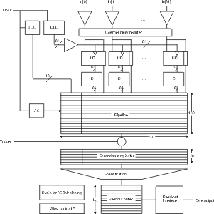
When used in the LHCb Outer Tracker, which is a large Straw Tube Detector system, the chip's inputs are connected to a discriminator of the ASD family (Amplifier Shaper Discriminator chip designed by Mitch Newcomer from Pennsylvania University). The output of the ASD is sampled with the time resolution of the TDC, i. e. 25ns/64 = 390ps. Every clock cycle, i. e. every 25ns, the first 0-1 transition (which is called a hit) of the sample is binary encoded and stored into a ring buffer of 160 stages. Hence, one hit can be detected within a time interval of 25ns. Since this is well below the intrinsic dead time of the ASDblr chip, no dead time is introduced by the OTIS chip at this stage.
The data for each of the 32 channels consists of a single bit, indicating the presence of a hit, and a 6 bit fine time, which is the drift time of the electrons in the straw tube in case there was a hit. This information is overwritten by new data after 160 clock cycles. If a so called trigger signal arrives a clock cycle earlier the data are transferred into a derandomizing buffer from which it is read out again to a read-out buffer. During transfer of data from the derandomizing buffer into the read-out buffer, the data are optionally zero supressed. This may take some clock cycles per event but since the derandomizing buffer is 16 triggers deep, up to 16 consecutive triggers can be accepted before the chip starts to ignore them. The read-out buffer is used to compensate fluctuations in the trigger rate in case the avaialable read-out data bandwidth is tight.
Data are transported of the chip via a simple parallel bus interface. This enables a simple connection of the OTIS chip to other chips that forward data to the next stages of the experiment. At the LHCb Outer Tracker the GOL chip, designed by Paulo Moreira at CERN, is foreseen, which has a 32bit parallel data bus interface. 4 OTIS chips are connected via 8bit lines each to one GOL chip. That means that each OTIS chip gets a fourth of the bandwidth of the GOL, which is 1.2Gbit/s effective. Hence each OTIS has 300Mbit/s available.
The OTIS has an I2C interface for slow control programming and monitoring. It can be connected to any system that makes I2C available, e. g. the SPACbus system. The OTIS not only can be programmed and monitored by this interface, but it also provides service for the ASD chip, by having 4 D/A converters on chip, which can be used to provide individually programmable threshold voltages for each ASD chip.